We have professional design & manufacturing staff with more than 10 years of experience. We offer following services for Electronic design requirements.
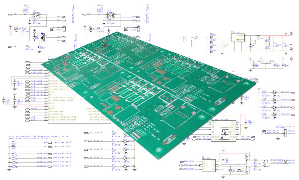
Our PCB layout and PCB design services and capabilities includes:
Single-sided, double-sided, and multi-layer boards (up to 16 layers) with high density design handing capabilities.
Component Library creation as per IPC standard.
Design for Surface mount, through-hole & mixed technology with QFN,BGA, PGA & fine pitch components.
Design as per EMI/EMC requirement.
Design for manufacturability (DFM)
Design for Assembly (DFA)
Bill of material generation.
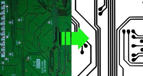
Reverse Engineering (Bare board to design file/Gerber)
Gerber generation
Stack up creation for multilayer.
PCB CAM Validation (SS, DS & ML up to 16layers)
Gerber RS274D to RS274X file format conversion.
Design/Manufacturer rule checking (DRC/MRC)
Complete Gerber database validation for manufacturability.
PCB Panelization as per DFM/DFA requirement.
NC drill program generation & optimization.
Rout Master program generation.
BBT program generation as per Machine compatibility.
Glue & Paste Stencil design as per SMT requirement.

 Antium Designer